GaN-Highpower

Research project at a glance

Period
01.05.2021 to 30.04.2024
Project Description
The field of photovoltaics has been subject to enormous price pressure for many years, as falling feed-in tariffs worldwide make low component prices necessary to be able to manufacture and operate a PV system economically. At the same time, the demands on the functional diversity of the devices continue to increase (e.g. universal use in PV and battery applications, grid feeding, self-consumption and island operation, provision of grid services).
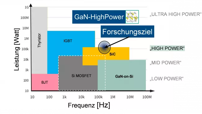
The goal of the GaN-HighPower collaborative research project is to explore and test the next generation of cost-effective, resource-efficient power converters for photovoltaic applications, with a focus on string inverters with higher power in the range above 100 kVA. For this purpose, gallium nitride (GaN) semiconductor modules together with application-oriented strongly improved inductive components and current sensors are to be researched and tested. Until now, the application of GaN technology has been limited to much lower power ranges. Within the scope of the project, the higher power range is to be opened up for PV through application-oriented research.

In this project, the Bonn-Rhein-Sieg University of Applied Sciences will support the pre-selection of topologies to be considered for the project with the help of suitable simulations and modeling. The focus is on the behavior of fast-switching GaN semiconductor modules, which will be developed by Infineon during the course of the project. These novel modules will be characterized by the university on a test bench specially developed in the project in order to make precise statements about the switching behavior at different operating points. The knowledge of the switching behavior enables an optimal tuning of the components, such as the gate driver to the semiconductor module in order to achieve the maximum efficiency and performance in the later PV and battery inverter. Another main task of H-BRS is the design and simulation of these gate drivers adapted to the novel GaN semiconductor modules and their associated power supply, as well as the design of the DC bus. The fast switching transients of the semiconductor modules place special demands on the control electronics in order to make optimal use of the advantages of GaN technology in the next generation of high-power PV and battery inverters.
In addition to the hardware, the university will implement the control and operation management using a processor suitable for the high switching frequencies and validate it through simulations and using the developed functional model/demonstrator to ensure efficient and optimal operation of the GaN inverter.
Cooperation partners


Sponsors


